Solar Cell Diagnostics by Combination of Kelvin Probe Force Microscopy with Local Photoexitation
A.V.Ankudinov Ioffe Physical-Technical Institute of the Russian Academy of Science National Research University of Information Technologies, Mechanics and Optics
Application Note 091
(pdf 2.6 Mb)
INTRODUCTION
The Sun is an abundant, easily accessible power source that is currently underutilized, will possibly become the no-alternative choice for electrical power of humankind [1]. It is believed that the most promising way to convert solar power is by the photoelectric method used in solar cells (SCs) [2]. The energy program of the European Union envisions that no less than 3% of electric power will be provided from solar installations by 2020 [3].
In the United States, the Solar America Initiative program anticipates that the volume of the “photovoltaic” market will already be $5-10 billion by 2015, with an increase to $20-30 billion by 2030 [4]. Interestingly, the factor hindering more intense development of the SC market is the high cost per Megawatt of produced electricity, rather than the energy conversion efficiency of SCs.
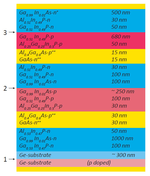
Fig.1. Schematic of an MJSC with three subcells. Designations: various tints of pink, p-type layers of the heterostructure; lightbluetints, n‑typelayers; and yellow, highly conducting layers of tunnel diodes and contact layers. The digits show the p-njunctions inthesubcells based on (1) Ge, (2) GaAs, and (3) GaInP2
FORMULATION OF THE PROBLEM
At present, the highest efficiencies, some exceeding 40%, are exhibited by multijunction (MJ) SCs based on semiconductor nanoheterostructures [5]. MJ SCs consist of several subcells with p-n junctions and barrier layers of various semiconductor materials.
These subcells are arranged in order of decreasing energy bandgaps from the photosensitive surface to the substrate, being linked by oppositely connected tunnel diodes. Each subcell converts into electricity the energy of the short-wavelength part of the incident spectrum and transmits its long-wavelength part to the next subcell. Thus, the energy of the whole solar spectrum is segmented and collected, resulting in high efficiencies. It is, however, important to note that the most inefficient subcell determines the overall efficiency of an MJ SC. Diagnostics of the constituent layers of such a composite device is commonly made using indirect, integral measurement techniques and mathematical simulation (see, e. g., [6]). Information obtained this way is not always unambiguous because it requires the solution of multivariate inverse problems. An unambiguous determination of the weakest segment will likely require separate monitoring of the operation of all the constituent subcells. (From the standpoint of circuitry, it is necessary to find the least efficient element in a set of se ries-connected photodiodes).
EXPERIMENTAL RESULTS AND DISCUSSION
Below is considered an example of how the NTEGRA Spectra «AFM – confocal – Raman – fluorescence» Probe NanoLaboratory (PNL) is used to study MJ SCs based on a GaInP2/GaAs/Ge heterostructure with three p-n junctions. The total number of layers exceeds 20, and individual layers less than 20 nm thick (see Fig. 1). The method of Kelvin probe force microscopy (KPFM) was used to measure the surface potential profile variations of a cross-section-cleaved SC in relation to the intensity, wavelength, and beam position of a laser excitation source. According to the schematic of the layers in Fig. 1, the distance between the p-n junctions of neighboring subcells based on GaAs and GaInP2 is shorter than a micrometer. The monitoring of the response, surface potential variation, of a separate subcell was enabled by focusing the excitation laser into a submicrometer spot. An objective with a numerical aperture of 0.7 and resolving power of 400 nm, was used in the confocal laser microscope integrated in the NTEGRA Spectra PNL. An AFM cantilever is positioned below the objective allowing simultaneous optical excitation and AFM measurements (Fig. 2b).
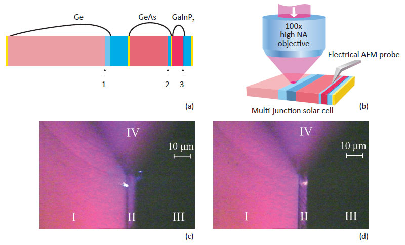
Fig. 2. (a) Schematic of layers in an MJ SC with the same color designations as those in Fig.1. The three p-n junctionsare shown by arrows. (b) Schematic of experiment. Optical micrographs of the edge of the cleaved surface of a SC during a KPFM experiment under focused photoexcitation of (c) the p-n junction in Ge with ablue laser (473 nm) and (d) p-n junction in GaAs with a red laser (785 nm). Latin numerals designate: (I) Ge substrate, (II) III-V layers (GaAs and GaInP), (III) free space, and (IV) KPFM cantilever. The optical microscopeis focused on the Ge substrate in Fig. 2c, and on the III-V layers in Fig.2d
Importantly, the instrument allows both independent and synchronized scanning of laser spot (using piezo- driven mirror) and the sample (using a sample piezo-scanner). Figures 2c and 2d show optical micrographs of cleaved surfaces of an MJ SC during an experiment. Near the edge of cleaved surfaces, spots of light from blue and red lasers focused on the p-n junctions can be seen in the subcells of Ge and GaAs, respectively. A topographic image and a map of the contact potential difference signal in the region in which the main MJ SC layers are located is shown in Fig. 3. The left half of the topographic image in Fig. 3a shows a sharp change in the surface topology. In this region, the smooth relief of the Ge substrate (situated on the left) abruptly changes to the striated topology of the III-V layers.
The significant difference between the topographies of Ge and III-V layers is also seen in the optical micrographs in Figs. 2b and 2c. Crystals of III–V materials are easily cleaved to form perfectly planar and atomically smooth surface, but only along {110} basal planes. This intrinsic property is, for example, used in the fabrication of mirrors for injection lasers based on III-V compounds [7]. Cr ystals of Ge (and also Si) pr eferentially cleave along different crystal planes.
The Ge substrate is two orders of magnitude thicker than all the other layers in the MJ SC, and therefore, cleavage propagation directions are predominantly based on the substrate. The cleaved Ge surface is significantly non-coincident with the basal plane of III-V layers. It is this lack of coincidence that leads to the formation of the strongly visible stepped topography on the cleaved surface of III-V la yers.
The map of the contact potential difference (CPD) in Fig. 3b shows features in good agreement with the expected built-in potential differences in the bulk heterostructure under full darkness conditions. The model profile of the built-in potential is shown in Fig. 3c above the schematic of layers of the heterostructure.
The small potential drops across thin tunnel-transparent layers are disregarded and the simulation describes a smoothed variation of the potential. The CPD map, however, shows that near the p-n junction on the surface of the GaAs subcell, there is only a subsequent decrease in the CPD signal instead of the expected peak (see Fig. 3c).
The variation of the built-in potential, see Fig. 3c marker 1, is not observed the light band region in the image in Fig. 3b. The light band region corresponds to well- doped transition layers between Ge and the GaAs subcell. These discrepancies occur because the surface potential of the semiconductor structure differs from the potential in the bulk by the amount of near- surface band bending, which is not known for an arbitrarily cleaved sample. The best agreement between the results of simulation and the experimental data can be achieved by studying distributions of the external voltage applied to contacts of the structure [8, 9] and surface photovoltage (SPV) distributions [10].
Below, the second case is analyzed in more detail. When the semiconductor surface is exposed to light with a photon energy exceeding the energy bandgap of the material, the separation of photocarriers by the near-surface field results in minority carriers emerging at the surface, which makes the band bending smaller [11]. This mechanism is operative for semiconductors with surfaces depleted of majority carriers, in which the surface photovoltage has the opposite sign to that of majority carriers.
In a complex structure, photocarriers can be separated not only in the near- surface field, but also in the bulk due to the field of built-in barriers. For example, it is possible to predict changes in the surface potential upon illumination of a single p-n junction.
Because of the photocarrier separation in the near-surface field, the p side is charged negatively, and the n side positively. By contrast, the separation of photocarriers in bulk material from the field of the p-n junction charges the p side positively, and the n side negatively.
If, for example, the number of photocarriers separated in the field of the p-n junction exceed those separated in the near-surface field, then the surface photovoltage will decrease, passing from the p side to the n side. If the contacts to the p and n sides are shorted, then the contribution from the bulk separation is eliminated, and the surface photovoltage will increase upon such a transition. Qualitatively, the photovoltage profile can be simulated in the same way in more complex compound structures, such as MJ SCs.
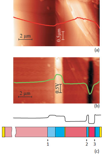
Fig.3. KPFM study of the cleaved surface of an MJ SC in the dark. During measurements both contacts to the MJ SC were grounded. (a) Topographic image of the cleaved surface profile, measured in intermittent contact mode (the color-scale contrast spans the height variations of 0.85 μm). (b) Map of the CPD signal measured in the second pass in the absence of an external photoexcitation (the color-scale contrast spans the CPD variations of 1.05 V). (c) Smoothed equilibrium profile of the built-in potential (from model). Schematic of the layers: arrows with digits show the p-n junction positions in the subcells (see also color designations in Fig. 1). Measurement parameters: AFM laser with a wavelength of 650 nm used in the system for cantilever deflection detection, noncontact VIT_Pprobe, resonance at 257 kHz, surface potential signal was measured at 100 nm lift height and Uac = 2 V
Figure 4 shows two sets of simulated and measured photovoltage profiles from a cleaved surface in alternate photoexcitation of p-n junctions in three subcells of MJ SCs.
The first set, Figs. 4a-4c, was obtained with blue laser excitation (wavelength λ = 473 nm), and the second, Figs. 4d-4f, with red laser excitation (λ = 785 nm).
The photoexcitation densities were approximately the same in both cases, 2-3 mW/μm2. The focal spot diameter D was calculated using the Rayleigh criterion D = 1.22 λ/NA, where λ is the laser wavelength, and NA = 0.7 is the numerical aperture of the objective.
The surface photovoltage profile was determined by the difference of CPD values measured under photoexcitation and in the dark. The simulation process, as described in the preceding paragraph, was performed with the following conditions; the contacts to the MJ SC are shorted,the photovoltage appearing in the bulk of a p-n junction exposed to light is distributed among the barriers of two nonilluminated p-n junctions.
For simplicity, the capacitances of these two junctions are considered to be equivalent. The light from the blue laser is absorbed by all layers in the MJ SC and light from the red laser is not absorbed by the wide- bandgap GaInP2 layers. The photoexcitation intensity gradually decreases away from the focusing region.
In the experimental photovoltage profiles, the arrows show a dip in Fig. 4b and a peak in Fig. 4c. The simulation also predicts these specific features. The mechanism of their appearance is discussed in more detail below.
The GaAs subcell is insulated from the contacts to the MJ SC by the potential barriers at the p-n junctions of the neighboring subcells. If it is exposed to blue light, separation of photocarriers in the field of the p-n junction results in electrons ejected into the n layers of this subcell. For this reason, a negative potential appears in the bulk of these n layers and in the p layers of the GaInP2 subcell.
Because of the photocarrier separation in the near- surface field, the surface of the p layers is also negatively charged relative to the bulk. The joint effect of both processes forms a deep dip in the surface photovoltage profile when it passes across the p layers of the GaInP2 subcell, as seen in Fig. 4b.
If blue light is replaced with red light, no photocarriers are generated in the wide-bandgap GaInP2 layers. As a result, the dip should be less pronounced, which is indeed observed in Fig. 4e. When the GaInP2 subcell is exposed to blue light, a positive potential appears in the bulk of its p layers and is transferred to the n layers of the GaAs subcell.
The photoeffect at the surface of the n layers is also positive, and a peak corresponding to these layers appears in the photovoltage profile (Fig. 4c). These considerations are helpful in the qualitative explanation of the shape of all of the profile curves.
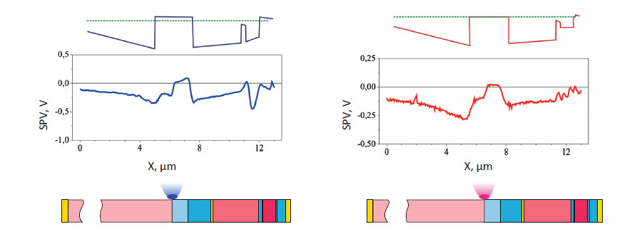
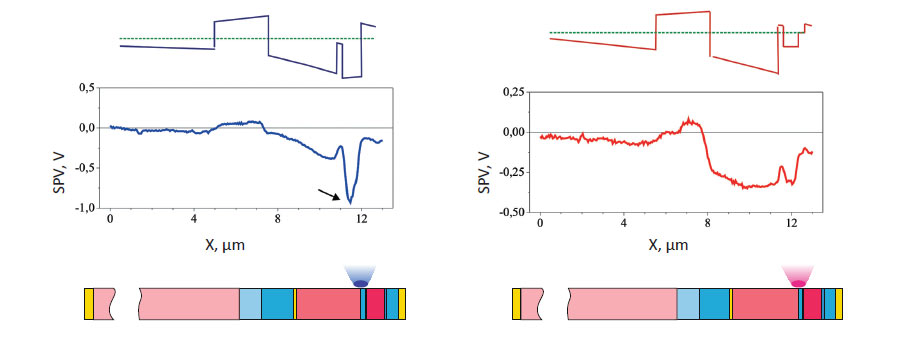
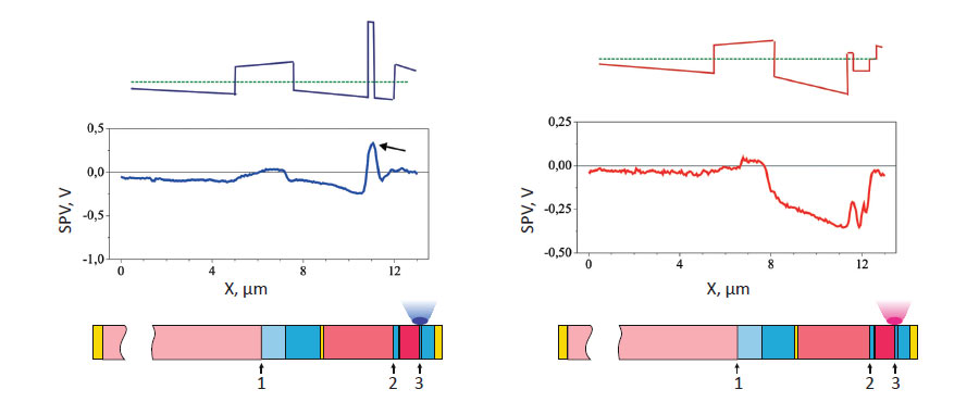
Fig. 4. Comparison of experimental and simulated data. (a-c) Photoexcitation with laser light (λ = 473 nm) focused on the p-n junctionsin (a) Ge, (b) GaAs, and (c) GaInP2. (d-f) Photoexcitation with laser light (λ = 785 nm) focused on the p-n junctions in (d) Ge, (e) GaAs, and (f) GaInP2. Designations: SPV, experimental surface photovoltage profile. A simulated profile is also given above each plot. Below, under all the plots are shown schematics of layers in MJ SCs (with the same color designations as those in Figs. 1-3). Comparison of the experimental and simulated data. (a-c) Photoexcitation with laser light (λ = 473 nm) focused
CONCLUSIONS
The study of a solar cell with three subcells based on Ge, GaAs, and GaInP2 in a NTEGRA Spectra PNL demonstrated that operation of each subcell could be separately monitored. The experimental surface- photovoltage profiles obtained are in good agreement with results of the qualitative simulation. The agreement between the simulation results and experimental data also indicates that there are no parasitic barriers in the multijunction solar cell under study for the chosen photoexcitation densities.
It should be noted that the NTEGRA Spectra PNL, integrating AFM with confocal optical spectroscopy techniques, offers a substantially broader set of capabilities for solar cell diagnostics than that considered in the present communication. The NTEGRA Spectra PNL provides the following measurement techniques with submicrometer and nanometer spatial resolution: surface topography; local conductivity; variations of potentials and charges, built-in or induced by external bias or photoexcitation; evaluation of compositional homogeneity and material defects; spatial and spectral variations of transmittance, reflectance, and other optical properties; localization of nonradiative recombination regions; monitoring of p-n junction positions; monitoring of heterointerface transitions; and mapping of mechanical stresses. All of these measurement scan be used to optimize the solar cell technology. For example, the internal design of solar cells can be optimized via correlation of regions having the maximum photovoltaic conversion efficiency with data on variation of the chemical composition, layer thickness, profile, defects, optical parameters, etc.
ACNOWLEDGMENTS
The author is grateful to his colleagues at the Ioffe Institute: V. M. Lantratov for the MJ SC samples he provided, A. S. Gudovskikh for assistance in simulating the built-in potential profile in a sample, and M.S. Dunaevskiy for helpful remarks on presentation of the results. Many thanks for skillful measurements to Artem Shelaev and Pavel Dorozhkin from NT‑MDT SI.
REFERENCES
[1] Zh. I. Alferov, V. M. Andreev and V. D. Rumyantsev. Solar photovoltaics: Trends and prospects. Semiconductors, 38(8), pp. 899-908 (2004)
[2] S. M. Sze. Kwo K. Ng. Physics of semiconductor devices. Chapter 13. Photodetectors and Solar Cells. Third eition. Wiley, N.Y. (2007).
[3] http://www.eupvplatform.org/publications/ strategic-research-agenda-implementation-plan. html#c2643
[4] http://www.eere.energy.gov/solar/solar_ america
[5] Karam N. H., Sherif R. A. and King R. R. //Springer Ser. In Opt. Sci. 2007 Vol.130 .P.199–219.
[6] S. A. Mintairov, V. M. Andreev, V. M. Emelyanov, N. A. Kalyuzhnyy and N. K. Timoshina, M. Z. Shwarz, V. M. Lantratov. Study of minority carrier diffusion lengths in photoactive layers of multijunction solar cells. Semiconductors 44(8), pp. 1084-1089 (2010).
[7] C. Casey, Jr. and M. B. Panish, Heterostructure Lasers, Academic Press, 1978.
[8] S. B. Kuntze, D. Ban, E. H. Sargent, St. J. Dixon- Warren, J. K. Whiteand, K. Hinzer. Electrical Scanning Probe Microscopy: Investigating the Inner Workings of Electronic and Optoelectronic Devices. Critical Reviews in Solid State and Materials Sciences, 30, 71‑124, 2005.
[9] A. V. Ankudinov, V. P. Evtikhiev, E. Yu. Kotelnikov, A. N. Titkov and R. Laiho. Voltage distributions and nonoptical catastrophic mirror degradation in high power InGaAs/AlGaAs/GaAs lasers studied by Kelvin probe force microscopy. J. Appl. Phys. 93, 432-438 (2003).
[10] D. K. Schroder. Surface voltage and surface photovoltage: history, theory and applications. Meas. Sci. Technol. 12, R16–R31 (2001).
[11] L. Kronik, Y. Shapira. Surface photovoltage phenomena: theory, experiment, and applications. Surface Science Reports 37, 1-206 (1999).

