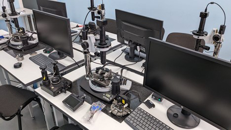
NTEGRA ACADEMIA

NTEGRA ACADEMIA

NTEGRA Academia is a multifunctional device for teaching high school children and university students the basics of scanning probe microscopy, including the participation in research projects in the field of nanotechnology, physics, chemistry, biology, medicine etc.

GENERAL INFORMATION

NTEGRA Academia is a multifunctional device for teaching high school children and university students the basics of scanning probe microscopy, including the participation in research projects in the field of nanotechnology, physics, chemistry, biology, medicine etc. The device is capable of performing more than 40 measuring methods, what allows analyzing physical and chemical properties of the surface with high precision and resolution. It is possible to carry out experiments not only by conventional silicon cantilevers but also by tungsten wire which is chiper and easy to use in educational proposes.

Special device for the tangsten probes creation by the method of electrochemical etching which allows to sharpen tangten probes by students themselves.

Exchangeable scanner with capacitive sensors with a scan range in high voltage mode (X × Y × Z); 100х100х10 microns, in the low voltage mode (X × Y × Z); 3x3x2 microns Minimum scanning step: 2 nm.

Nova SPM software for high efficiency SPM control and image processing.

The new generation electronics provides operations in high-frequency (up to 5MHz) modes. This feature appears to be principal for the work with high-frequency AFM modes and using high-frequency cantilevers.*


APPLICATIONS

  • Biology and Biotechnology
    Proteins, DNA, viruses, bacteriums, tissues
  • Materials Science
    Surface morphology, surface morphology, local piezoelectric properties, local adhesion properties, local tribological properties
  • Magnetic materials
    Magnetic domain structure visualization, observation of magnetization reversal processes that depend on external magnetic field, observation of magnetization reversal processes under different temperatures
  • Semiconductors, electric measurements
    Wafers and other structures morphology, local surface potential and capacitance measurements, electric domain structure imaging, determination of heterojunction bounds and semiconductor regions with different doping levels, failure analysis (localization of conductor line failure and leakage in dielectric layers)
  • Polymers and Thin Organic Films
    Spherulites and dendrites, polymer monocrystals, polymer nanoparticles, LB-films, thin organic films
  • Data storage devices and medias
    CD, DVD disks, storages for terabit memories with thermomechanical, electric and other types of recording
  • Nanomaterials
    Nanopowders, nanocomposites, nanoporous materials
  • Nanostructures
    Fullerenes, nanotubes, nanofilaments, nanocapsules
  • Nanoelectronics
    Quantum dots, nanowires, quantum structures
  • Nanomachining
    AFM lithography: force (ac and dc), current (Local anodic oxidation), STM lithography
  • Nanomanipulations
    Contact force

SPECIFICATIONS

Measuring modes and techniques

Training Head Scientific Head
– AFM semi-contact
– Phase Imaging
– STM Constant Current mode
– STM Constant Height mode
– Force spectroscopy
– Dynamic force nanolithography
– Oxidation nanolithography
– Contact AFM
– Contact AFM
– Lateral force microscopy
– Electrostatic Force Microscopy
– Scanning spreading resistance microscopy
– Force modulation microscopy
– Piezoresponce force microscopy
– Semicontact AFM
– Phase imaging
– Force-distance spectroscopy
– Dynamic force nanolithography
– Amplitude-distance spectroscopy
– Oxidation nanolithography
– AFM Lithography – Dynamic Plowing
– Phase-distance spectroscopy
– Frequency-distance spectroscopy
– Force-volume mode
– Electrostatic force microscopy
– Scanning capacitance microscopy
– Kelvin probe force microscopy
– DC Magnetic force microscopy
– AC Magnetic force microscopy

TECHNICAL DATA

Scan type Scanning by sample Scanning by probe*
Sample size Up to 40 mm in diameter,
to 15 mm in height
Up to 100 mm in diameter,
up to 15 mm in height
Sample weight Up to 100 g Up to 300 g
XY sample positiniong 5×5 mm 5×5 mm
Positioning resolution readable resolution – 5 um
sensitivity – 2 um
readable resolution – 5 um
sensitivity – 2 um
Scan range 100x100x10 um
3x3x2,6 um
Less than 1x1x1 um
100x100x10 um
50x50x5 um
Scan range Up to 200x200x20 um**(DualScanTM mode) Up to 200x200x20 um**(DualScanTM mode)
Non linearity, XY
(with closed loop sensors)
≤0.1% ≤0.15%
Noise level, Z
(RMS in bandwidth 1000 Hz)
With sensors 0.04 nm (typically),
≤0.06 nm
0.06 nm (typically),
≤0.07 nm
Noise level, Z
(RMS in bandwidth 1000 Hz)
Without sensors 0.03 nm 0.05 nm
Noise level, XY*** >
(RMS in bandwidth 200 Hz)
With sensors 0.2 nm (typically),
≤0.3 nm (XY 100 um)
0.1 nm (typically),
≤0.2 nm (XY 50 um)
Noise level, XY*** >
(RMS in bandwidth 200 Hz)
Without sensors 0.02 nm (XY 100 um),
0.001 nm (XY 3 um)
0.01 nm (XY 50 um)
Linear dimension estimation error
(with sensors)
± 0.5% ± 1.2%
Optical viewing system Optical resolution 1 um
(0.4 um optional, NA 0.7)****
3 um
Optical viewing system Field of view 4.5-0.4 mm 2.0-0.4 mm
Optical viewing system Continuous zoom available available
Vibration isolation Active 0.7-1000 Hz 0.7-1000 Hz
Vibration isolation Passive above 1 kHz above 1 kHz

* Scanning head can be configured to serve as a stand-alone device for specimens of unlimited sizes.
** Optionally can be expanded to 200x200x20 мm.
*** Built-in capacitive sensors have extremely low noise and any area down to 50×50 nm can be scanned with closed-loop control.
**** High Resolution Viewing system (HRV head) is optional and provides additional functionality making it possible to generate and detect tip-localized aperture less near-field effects.


ASK YOUR QUESTION: