
NTEGRA THZ
THz near-field imaging system (sSNOM).
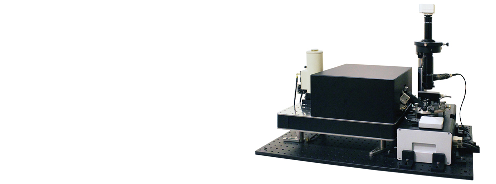
THz near-field microscope has been developed together with a new generation of NTEGRA system. We utilize the high-power laser to generate a stable THz pulse train. Single-cycle THz pulses with THz electric fields and a 0.15 – 5 THz spectral width can be generated with the photoconductive antenna system. The THz beam is focused down to a ~600 μm spot under the AFM tip which yield scattering-type THz near-field signal with < 50 nm spatial resolution. The THz near-field system is also equipped with built-in heating stage and purge box, capable of studying high-temperature THz near-field spectroscopy with different gaseous environment.
SCHEMATIC OF THE NEAR FIELD OPTICAL-PUMP THZ-PROBE (N-OPTP) SETUP
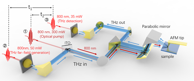
Figure 1: Schematic of the near field optical-pump THz-probe (n-OPTP) setup, equally capable of performing optical pump near-field THz emission (n-OPTE) experiments. ①: 800 nm, 300 mW pump pulses pass through the ITO and collimate with the THz beam ②. Optical pump ① and THz probe ② are focused onto the AFM tip apex using an off-axis parabolic mirror. ③: THz gate (detection) beam. Tip scattered THz signals can be mapped out in the time domain by changing the time delay between ② and ③ (t1). Changing the delay between ① and ③ (t2) probes the photo-excited ultrafast dynamics of the sample. When t1 is fixed at the peak position of the scattered THz electric field while t2 is varied, n-OPTE (with THz probe ② blocked) and n-OPTP (with THz probe ② unblocked) can be performed.
SPECIFICATIONS
Far-field THz performance:
| Excitation Laser | Laser central wavelength 800 nm +/- 50 nm, pulse length < 120 fs, average power > 100 mW; time synchronized with the THz pulses |
| Measurement Modalities | Transmission & Reflection |
| Average Optical Power on Transmitter | >15 mW |
| Average Optical Power on Receiver | >15 mW |
| Bias Voltage on Transmitter | ± 60V square wave |
| Terahertz Peak Measured Photocurrent | >2 nA high BW; >30 nA high signal |
| Terahertz Spectrum Bandwidth | >5 THz high BW; >4 THz high signal |
| Power Spectrum Dynamic Range | >70 dB high BW; > 80 dB high signal |
| Typical Scan Time | 2-5 min |
Dry air purge box
Imaging raster scan hardware and software
Lock-in amplifier and Low-Noise current Amplifier
Far-field THz performance:
The basic laser and scanning scheme are the sample as the far-field setup.
| Near-field THz spectral range: | 0.3- 2 THz |
| Near-field THz signal to noise: | S2 20:1 at 30ms lock-in integration time |
| Typical Scan Time | 15-60 min |
Dry air purge box
Near-field Image taken in integrated NT-MDT AFM software
Optical pump THz probe compatible
THz near-field emission microscopy compatible
APPLICATION EXAMPLE
Using the THz near-field system, nano-imaging of micrometer size graphene samples on SiO2 (300 nm)/Si substrate were performed. The graphene was mechanically exfoliated onto PDMS (Polydimethylsiloxane) and dry transferred onto a prepatterned Au lead (30 nm thick). Here the Au lead is used for electrostatic gating and serves as a reference for graphene imaging. Figure 2a,b show the simultaneously collected AFM topography and near-field images with a size of 10 × 10 μm, respectively. As shown in Figure 2b, there is clearly a large optical contrast between single layer graphene (SLG, marked as 1) and the SiO2 substrate (marked as 0). However, no obvious contrasts between SLG and multilayer graphene can be observed (the multilayers are marked by the number of layers as 2, 3, 4, and 5+). Moreover, a comparison between single-layer graphene and a 30 nm gold film revealed comparable THz near-field signals (see Figure 2c,d). These observations suggest that monolayer graphene has close-to- perfect near-field THz reflection.31 This near-unity THz near- field reflectivity is found to be independent of the carrier density when the back-gate voltage is swept between ±30 V at room temperature (RT). To compare the THz near-field spectra between SiO2 and graphene, we plot the time domain signal in Figure 2e and the Fourier-transformed THz spectrum in Figure 2f. The normalized THz nanospectrum S2 (graphene)/S2 (SiO2) reveals that the near-field signal of graphene is 3−4× larger than that on the bare SiO2 over the 0.2−1 THz frequency range. In the inset of Figure 2f, the unnormalized spectra of graphene and SiO2 are plotted. A dip at about 0.75 THz can be observed, which was reported in previous THz near-field experiments. Since this dip is absent in the far-field THz measurements using the same optics but excluding the involvement of the AFM tip, it is considered to be caused by the complex tip-light interactions and can be an interesting point for further investigation.
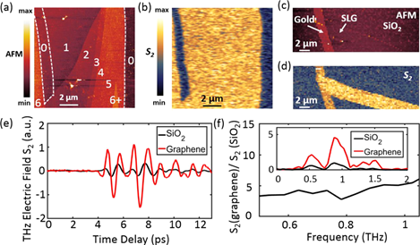
Figure 2: (a, b) AFM topography and THz near-field (S2) mapping of graphene on SiO2, respectively. The numbers of graphene layers are marked in (a), with bare SiO2 marked as 0. (c, d) AFM and THz near-field (S2) images of a SLG with a gold electrode. The near-field signal in graphene is comparable to that on the thin gold films. (e) Near field THz-TDS signal of SiO2 (black) and graphene (red). (f) Normalized graphene THz near- field spectrum (to SiO2). The inset shows a Fast Fourier Transform (FFT) of (e), which is the unnormalized S2 spectra of graphene (red) and SiO2 (black).
For more details please refer to Zhang, Jiawei, Chen, Xinzhong, et al. “Terahertz Nano-imaging of graphene.” ACS Photonics (2018).