
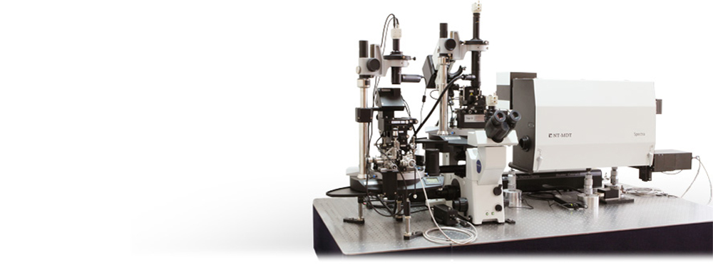
NTEGRA SNOM
Optical imaging and spectroscopy on the nano-scale.
General information
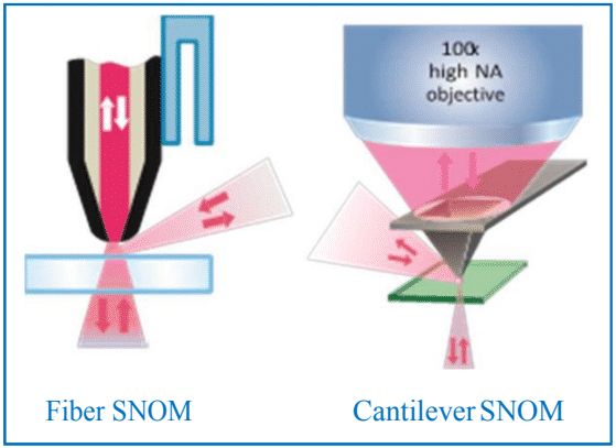
Scanning near-field optical microscopy (SNOM) enables studying a sample’s optical properties with resolution far beyond the diffraction limit. Sample fluorescence, light emission, transmission, scattering etc. can be mapped with the spatial resolution down to few tens nanometers. Two main approaches to the near-field microscopy exist: (i) aperture type SNOM and (ii) apertureless techniques.
In the first case, a subwavelength size aperture on a scanning tip is used as an optical probe. This is usually an opening in a metal coating of either an optical fiber tip or of a cantilever. Spatial resolution in the aperture type SNOM is, in general, determined by the aperture diameter. Apertureless techniques are based on the near-field optical phenomena as well, but do not require passing the light through an aperture. Apertureless/Scattering SNOM, Tip Enhanced Raman/Fluorescence, STM Light Emission and others fall into this category. SNOM techniques are widely used in nanophotonics (plasmonics, photonic crystals & waveguides etc.), laser technology, optical micro-devices and material science.
APPLICATIONS
- Laser emission;
- Optical fibers;
- Optical micro-devices;
- Plasmonics;
- Photonic crystals and waveguides;
- Photovoltaics;
- Quantum Dots.
BASIC SYSTEM CONFIGURATIONS
Fiber SNOM system
- Tip scanning (& sample scanning): important for plasmonics;
- Tuning fork Shear force tuning fork feedback provides stable positioning of the SNOM probe just a few nm away from the substrate;
- Tuning fork feedback does not need AFM laser. This allows to use fiber SNOM in a very wide optical range (Ultraviolet, Visible, Infrared) without any interference with AFM laser;
- SNOM Modes: Reflection, Collection, Transmission.
Cantilever SNOM system
- Cantilever SNOM probes are more reproducible, robust and have longer lifetime;
- Transmission of SNOM probe is higher that of fiber SNOM probe (for the same aperture size).
- AFM laser deflection feedback allows to use all different feedback modes: contact, semicontact, non-contact;
- Automated alignment (laser-to-aperture);
- SNOM Modes: Collection, Transmission.
SNOM FOR OPTICAL MICRO-DEVICES
Near-field focusing of a phase micro-fresnel zone plate
Focusing behavior of a binary phase micro- Fresnel zone plate (FZP) fabricated using focused ion beam milling on a glass substrate is studied by SNOM. It is found that an asymmetric spot with subwave-length beam width and elongated depth of focus can be obtained from the phase micro- FZP. The measure- ments are consistent withcalculation results.
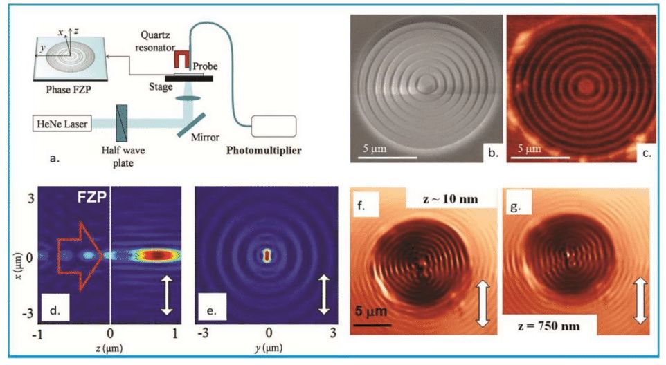
(a) Experimental setup. (b) SEM image and (c) shear-force topography of the phase micro-FZP. The phase plate has eight full zones with the etch depth about 300 nm. (d), (e) Calculated electric field intensity distribution of the incident and transmitted lights in XZ and XY plane. (f), (g) Experimental intensity distribution of the electric field intensity (detected by SNOM) after being transmitted through the phase micro-FZP at planes located at 10 nm and 750 nm height from the plate surface. Data from: R.G. Mote, S.F. Yu, A. Kumar, W. Zhou, X.F. Li, APPLIED PHYSICS B 102: 95–100 (2011).
Characterization of a micro-focusing plasmonic device
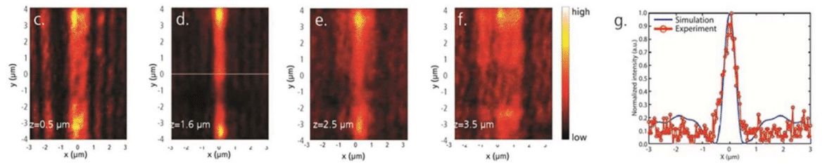
Focusing behavior of Au based focusing plasmonic device is characterized by SNOM. The experimental results show a significant focusing effect in agreement with the simulation results.
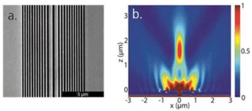
(a) SEM image of the device. (b) The electric field intensity distribution of the transmitted lights through the plasmonic device (simulated). The transmitted fields are detected with the SNOM. The intensity distribution of the transmitted lights at the horizontal planes with the distances of (c) z=0.5 μm, (d) z=1.6 μm, (e) z=2.5 μm, and (f) z=3.5 μm away from the device surface; (g) The intensity distribution along the solid line in (d). Data from: Dr. Fenghuan Hao, Dr. Rui Wang and Dr. Jia Wang , OPTICS EXPRESS Vol. 18, No. 3, 15741- 15746 (2010).
SNOM for photonic crystals
Light propagation in a photonic crystal waveguide
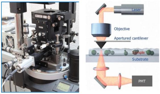
Aperture-SNOM in collection mode is used to correlate the electromagnetic field distribution with the surface topography of the photonic crystal. The optical near-field confined above the sample surface is collected by a SNOM tip, placed several nanometers above the sample surface.
Light propagation in a one-line-defect photonic crystal (PhC) waveguide patterned into a 450 nm thick free-standing lithium niobate membrane. SNOM topography (a) and optical near-field (b) images recorded above the surface of the PhC waveguide. The Bloch wave vectors of the PhC waveguide can be retrieved from optical near-field images.
Data from: R. Geiss, S. Diziain, N. Janunts, APPLIED PHYSICS LETTERS 97, 131109 (2010).Analysis of slow bloch modes in a photonic crystal
Analysis of slow bloch modes in a photonic crystal
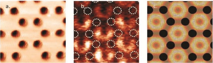
The photonic crystal is prepared by drilling a honeycomb lattice of air holes in the InP slab using e-beam lithography followed by reactive ion etching. Near-field optical microscopy is used to visualize the evanescent component of the mode with a spatial resolution below the diffraction limit.
(a) Shear-force topographic image (2×2 µm). (b) Optical near-field image at 1611 nm (2×2 µm), circles indicate holes positions of the 2D-Photonic crystal. Doughnut-shaped monopolar modes in each unit cell are observed, having the inner and outer radiuses 70 nm and 310 nm correspondingly. (c) Simulated electrical field intensity at the surface of the photonic crystal (2×2µm).
Data from: Thanh-Phong Vo, Adel Rahmani, Ali Belarouci, Christian Seassal, Dusan Nedeljkovic and Ségolène Callard, OPTICS EXPRESS Vol. 18, No. 3, 15741- 15746 (2010).
SNOM for plasmonics
Polarization-Controlled Tunable Directional Coupling of Surface Plasmon Polaritons
The polarization states of the optical signal that can be coupled to a plasmonic device are often limited by the selectivity of the coupling process. For directional SPP excitation, usually only the component of the incident light that is polarized perpendicularly to either groove- or ridge-like scattering elements (in the case of gratings) or to the metal surface itself (in the case of prism-based schemes) can be coupled into SPPs . Light in the orthogonal polarization does not couple to SPPs, leading to a decrease in the SPP signal and a loss of information about the incident polarization state.
Additional challenges arise in controlling the direction of propagation of the generated SPPs. Usually the direction of propagation of generated SPPs is difficult to control, that results in a substantial source of noise and reduces efficiency. This work presents a directional plasmonic coupler that addresses these challenges by offering polarization- invariant coupling efficiency to SPPs while allowing full control over the distribution of power between two counter-propagating SPP modes. This includes unidirectional coupling and preserves polarization information. A special structure was fabricated in a 150-nm-thick gold film using focused ion beam milling (FIB). The structure was backilluminated with polarized 633-nm laser light, and the SPPs were measured using scanning near-field optical microscopy.
Surface plasmon polaritons (SPP) formed by coupler structure: (a) SEM image of a structure fabricated in a gold film for operation at λ=633 nm. SNOM images of the structure backilluminated by light with different polarizations (b) linear, (c) right circular, (d) left circular.
Data from: Jiao Lin, J. P. Balthasar Mueller, Qian Wang, Guanghui Yuan, Nicholas Antoniou, Xiao-Cong Yuan, Federico Capasso, SCIENCE, Vol. 340 , 331-334 (2013).
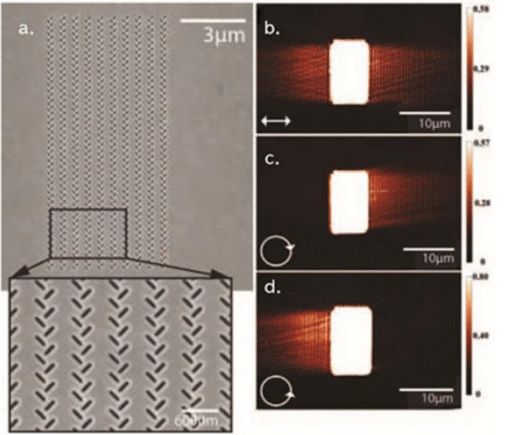
Guided plasmons on a gold waveguide
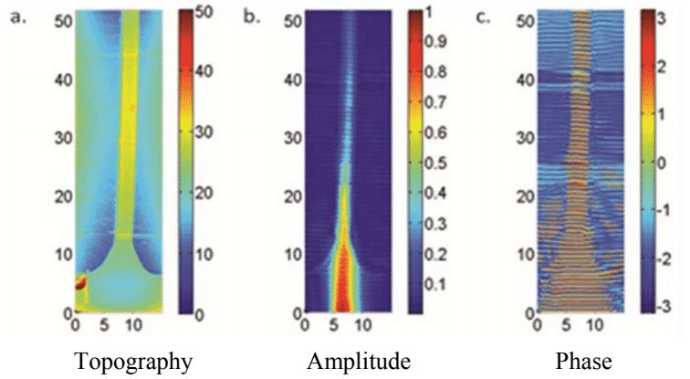
Surface plasmon polariton (SPP) propagation in an SPP waveguide is studied using SNOM equipped with aheterodyne interferometer. Both intensity and phase distribution of SPP electromagnetic field are measured.
(a) Topography of the waveguide. (b) Amplitude of the electromagnetic field coupled by SNOM probe. (c) Phase of the electromagnetic field. 785 nm excitation laser is used.
Data from: Antonello Nesci and Olivier J.F. Martin
Generation of plasmonic moiré fringes using phase-engineered optical vortex beam
The work demonstrates the dynamic generation of two dimensional (2D) plasmonic Moiré fringes resulting from the overlapping of two Surface Plasmon Polaritons (SPP) standing waves with an angular misalignment. The SPP waves are excited by an optical vortex (OV) beam with different topological charges (l= ±6). The sign of l determines handedness of the helical wave front. Due to their unique phase properties, OV beams provide a natural and simple phase modulation method to effectively and dynamically manipulate SPPs.
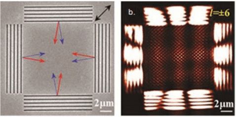
(a) SEM image of four metallic gratings to generate plasmonic Moiré fringes. Black arrow shows the polarization direction of incident optical vortex beam. Red and blue arrows show the propagation direction of SPP excited by positive and negative topological charge optical vortex beams, respectively. (b) SNOM measured Moiré fringes resulting from overlapping of the two SPP standing waves.
Data from: Guanghui Yuan, Qian Wang, and Xiaocong Yuan, OPTICS LETTERS, Vol. 37, No. 13, 2715-2717 (2012).
Scattering (apertureless-) SNOM
Scattering (apertureless) SNOM technique is usually used to visualize localized electromagnetic field in plasmonic structures. In this technique, a sharp probe is used to scatter localized near-field light into the far field. The scattered radiation intensity is measured in far field while tip scans over the sample surface, thus visualizing distribution of light localized in the structure with spatial resolution ~10 nm.
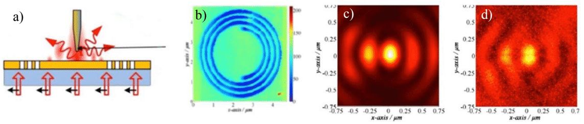
(a) Scattering SNOM is used to visualize longitudinal field distribution ( |Ez|2 ) in a plasmonic lens (PL). (b) AFM image of the PL structure – circle slits in a thin Au film on a glass substrate. (c) Calculated and (d) measured longitudinal field intensity in the center of the PL.
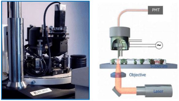
Snom imaging for laser studies
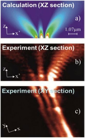
a) Simulation of XZ intensity distribution of the light emitted by 1.07 μm laser diode. b) XZ intensity distribution measured by cantilever based SNOM, c) XY intensity distribution of light emission measured at the laser surface in SNOM collection mode.
Data from: A. Shelaev, M. Yanul, P. Dorozhkin, NT-MDT. Sample courtesy: A. Ankudinov, S. Slipchenko, A. Podoskin, I. Tarasov, Ioffe Physical Technical Institute.
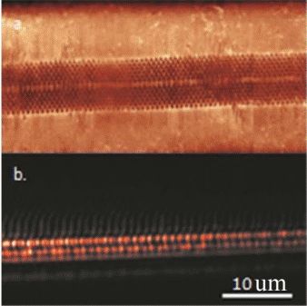
Photonic crystal optical fiber
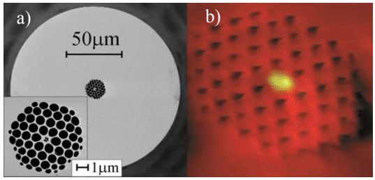
(a) SEM image of the optical fiber cross-section, showing photonic crystal structure in the fiber core. (b) Overlay of topography map (red palette) and light intensity (SNOM collection) image (green palette) taken from the fiber section. Light propagating in the fiber is perfectly localized in the center of the photonic crystal structure.
Data from: Chien-Chih Lai, Shih-Chang Wang, Yen-Sheng Lin, Ting-Hao Chen, and Sheng-Lung Huang, JOURNAL OF PHYSICAL CHEMESTRY C, 115, 20289– 20294 (2011).