
NTEGRA SPECTRA
Simultaneous and colocalized sample investigation by scanning probe microscopy & Raman microscopy/ spectroscopy methods.
Comprehensive physical & chemical analysis.
- Scanning probe microscopy (more than 40 measuring modes)
- Optical microscopy and confocal laser (Rayleigh) microscopy
- Confocal Raman microscopy
- Confocal fluorescent analysis – imaging and spectroscopy
- Scanning near-field optical microscopy (SNOM)
- Tip-enhanced Raman/ fluorescent spectroscopy (TERS, TEPL)
- Environmental control (temperature, liquid, electrochemical environment)
APPLICATIONS
Nano-materials
Polymers, organic films
Inorganic materials and minerals
Semiconductors
Microelectronics
Biology, medicine, pharmacy
HOW IT WORKS
Raman spectroscopy is a non-destructive, non-contact and fast method for physical and chemical analysis which does not require any special sample preparation. The method allows to analyze solid, liquid, powdery samples, gases, solutions, suspensions, etc. The signal can be taken through optically transparent media that have a very small Raman scattering cross section, e.g., polyethylene and other transparent polymers, glass. No vacuum or other special conditions are required for measurements, spectra are usually recorded at atmospheric environment and room temperature. If needed, the NTEGRA Spectra can optionally be operated in the widest range of temperatures, gas pressures.
In contrast to ordinary elastic (or Rayleigh) scattering, when the photon energy is not changed, Raman scattering is inelastic one. It involves both absorption of the photon and emission of the photon, with different energies. Its probability is very low compared to Rayleigh scattering process, and spectra registration requires the use of high-sensitive detectors. The key feature of the Raman effect is the fact that the energy difference between absorbed and emitted photons (or frequency shift) is exactly equal to the transition energy between the levels of the molecule. Thus, the spectral set of Raman shifts is a unique characteristic for each chemical compound, and works as a fingerprint of the molecule. The spectra obtained provide qualitative and quantitative information. Raman peaks positions indicate the chemical compound and its functional groups while the intensity indicates its concentration. An important information is also provided by shifts in peak positions with changes in temperature or pressure.
Together with infrared (IR) spectroscopy, Raman spectroscopy joins a group of techniques called vibrational spectroscopy. Both methods of spectroscopies study the same vibrational levels of molecules, but in different ways. Infrared spectrometers record absorption or emission spectra, while Raman spectrometers record inelastic light scattering. Both methods provide complementary information on the structure of complex molecules containing various functional groups. For example, Raman spectra reveal intense signals of nonpolar functional groups, double and triple carbon bonds, symmetrical vibrations of aromatic rings. In IR spectra, vibrations of polar substituents, in particular, hydroxyl, carbonyl and amino groups, are seen better.
Raman instruments typically use a dispersive monochromator with a diffraction grating and a multichannel spectral detector, and the source of incident photons for a Raman spectrometer is usually a laser. Since the Raman scattering cross-section is inversely proportional to the 4th grade of the wavelength, and the most effective multichannel detectors for the spectrometer today are silicon CCDs with the red limit of the operating range ~ 900 nm, it is optimal to use lasers from near-UV to near-IR (200 – 800 nm).
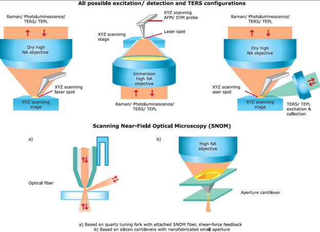
Confocal Raman/ fluorescence microscopy
- Confocality principle – spatial filtering of the collected optical signal through a small diameter aperture
- Two main confocal modes arescanning by laser and scanning by sample
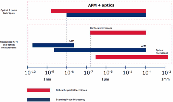
- Ultimate optical resolution; in the visible wavelength range up to 200 nm in XY and up to 400 nm in Z
- 3D chemical & structural information through Raman & Fluorescence mapping
Well-known disadvantages of Raman microspectroscopy are the diffraction-limited spatial resolution and poor level of the Raman signal (e.g., with respect to the photoluminescence signal). To evade these obstacles, the effect of localization of the electromagnetic field energy density near small conductive particles or metallic irregularities on the nanometer scale and the significant enhancement of the response in the emission spectrum due to “nanoantenna” effect have been actively investigated in recent decades. This phenomenon is known as giant Raman scattering (GRS). When the amplified signal is coming from beneath of the microscope probe tip (STM needle, AFM cantilever, etc.), we speak of tip-enhanced Raman scattering (TERS) and tip-enhanced photoluminescence (TEPL) spectra.
Optical microscopy/ spectroscopy with subwavelength spatial resolution due to tip-enhancement.
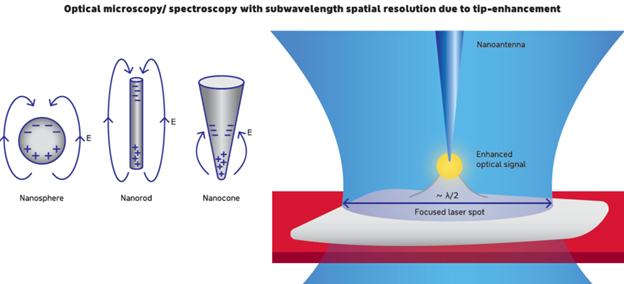
- An acute metal probe (nanoantenna) is used to localize and to amplify the optical field underneath the tip
- Non-destructive scanning probe microscopy for topography measurements and other surface parameters characterization
- Microspectroscopy with nanometer resolution
The NTEGRA Spectra was the first commercially available probe-spectral instrument specifically designed for applications requiring significant enhancement of the microspectral emission signal.
The NTEGRA Spectra optical scheme provides the light-paths from the source to the probe and to the sample, and for recording the emission radiation, optimized in design to maximize the gain of the useful signal. The instrument can get the emission signal from a localized spot few nanometers in diameter on the sample surface directly under the probe tip. Even single molecules can be detected and recognized from their spectra this way. The lateral resolution of Raman (TERS) and photoluminescence (TEPL) maps taken by the NTEGRA Spectra is no longer restricted by the Abbe diffraction limit and can be less than 10 nm.
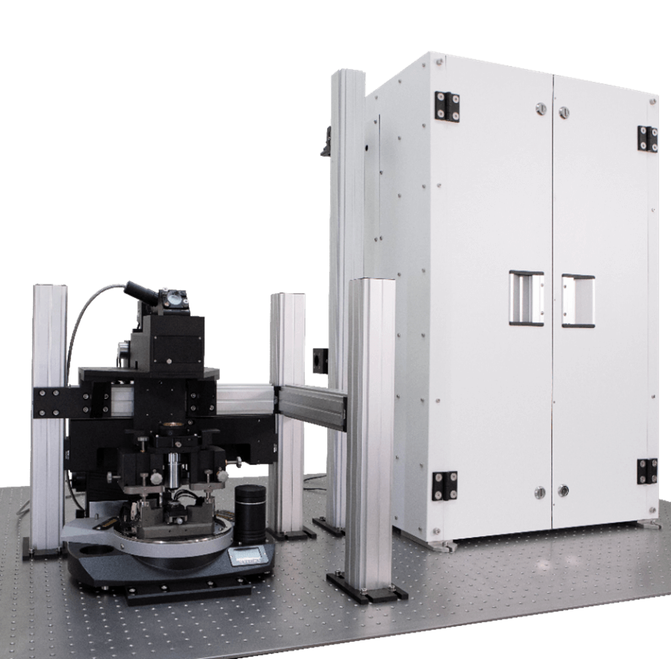
DESIGN
In order to get the complete information about the sample under investigation, a combination of several measurement techniques is often useful. The NTEGRA Spectra nanolaboratory is the world’s first full-featured integration of a scanning probe microscopy together with confocal Raman/ photoluminescence microscopy and spectroscopy.
The NTEGRA Spectra works in almost all of existing AFM and STM modes (more than 40), providing comprehensive information of the sample physical properties with nanometer resolution: local topography, stiffness, elasticity, conductivity, capacitance, magnetization, surface potential, friction, piezo response, etc. Different types of probe sensors can be used with the probe head.
Confocal photoluminescence and Raman measurements can be done simultaneously with SPM measurements on the same sample area providing information on the chemical compounds of the sample, its crystal structure, its orientation and deformation, impurities and defects, conformation of macromolecules, etc.
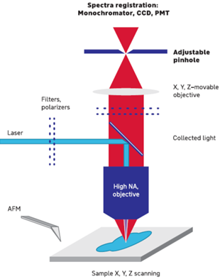
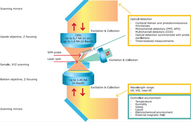
Three channels of the NTEGRA Spectra input/ output system allow to drive the excitation laser light onto the sample and to collect the emission signal via top, side and bottom optical channels. All three channels can be installed individually or simultaneously within the system.
The full Raman and/ or photoluminescence spectrum is recorded at each scan point, followed by a detailed software analysis. Due to the NTEGRA Spectra high performance, spectral maps of the emission signals coming from the sample can be obtained with spatial (both lateral and axial) resolution close to a theoretical limit.
The NTEGRA Spectra has a modular structure and allows to integrate different units within one instrument, satisfying almost all user’s needs. The design of the optical part permits replacing and adding laser sources, detectors, diffraction gratings according to the tasks of the experiment.
Installation of solid-state laser sources inside the spectrometer makes it possible to place the whole instrument on the optical table compactly. When changing the excitation laser, the excitation line cutoff filter, the neutral density filter (to control the laser power), the diffraction grating in the monochromator and the spectral detector, it is enough to select the appropriate units in the control panel, and the equipment will be reconfigured automatically.
The software also allows the automatic adjustment of the opto-mechanical elements to optimize the position of the confocal aperture, to adjust the position of the laser focus close to the probe, and to maximize the optical emission signal from the sample.
The optical microscopy unit in the NTEGRA Spectra allows to use different objective lenses, both dry (air) and immersion ones. Immersion lenses with apertures up to NA=1.45 can be used in the bottom optical channel. Dry lenses with apertures up to NA=0.7 can be used in the top optical channel simultaneously with probe measurements. Without a probe it is possible to use dry lenses with a larger aperture (up to NA=1.0) in the top channel.
Low magnification lenses (e.g., 10x) are usually used in the NTEGRA Spectra for visual control of the preliminary probe approach to the sample, for the selection of the scanning area on the sample, for the preliminary positioning of the tip end near the optical axis of the microscope.
High-aperture lenses are used for Raman and photoluminescence measurements, as well as for combined probe-optical experiments with high spatial resolution (e.g., for a 100x air objective, the typical lateral resolution is 0.4 µm for the visible spectral range). The high-aperture lenses also allow a precise control of the reconciliation of the laser spot and the probe tip, which is important for maximizing the probe amplification effects of the optical signal.
The optical scanning unit contains two software-controlled galvo-mirrors. Each mirror can be rotated by a small angle around one of the mutually perpendicular axes, to map quickly the sample surface by a laser beam and to take an emission signal from the surface point-by-point.
Various detectors are used to obtain the emission signal from the sample surface. A CCD camera is used to record the full spectrum or its part at each scan point (obtaining a full spectrum map). PMT or APD are used to accumulate and record the emission signal in a peculiar band of the spectrum and are useful for analyzing samples with a weak optical response.
Also, a separate PMT module is used for confocal laser microscopy in both top and bottom optical channels, with visualization of the sample optical properties contrast (absorption, reflection, transmission, scattering).
For colocalized measurements by simultaneous optical (spectral) and AFM methods, probes of a peculiar form are used, where the inclined needle protrudes beyond the cantilever visor.
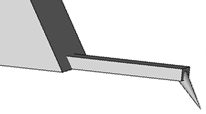
Probe tip for colocalized measurements
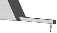
Standard AFM probe tip
OPTICAL MICROSPECTROSCOPY
NTEGRA Spectra is a confocal laser, Raman and photoluminescence microscope in its basic version. The instrument provides sample visualization, focusing of the excitation laser onto the sample and collecting of emission radiation coming from the sample. Micro-mapping can be accomplished by moving the sample and/ or moving the laser focus by means of galvo-mirrors.
The system in basic configuration provides:
- white light high-resolution optical image of the sample with full functionality of an upright or an inverted optical microscope;
- 2D image of the sample surface in laser confocal microscopy mode;
- 3D layer-by-layer optical image of a transparent sample in laser confocal microscopy mode;
- 2D and 3D Raman spectra mapping;
- 2D and 3D photoluminescence spectra mapping;
- photoluminescence maps with time-resolved measurements;
- spectral measurements, mapping, and sample imaging with light polarization control
SPM + OPTICAL MICRO-SPECTROSCOPY
NTEGRA Spectra in the extended version “probe microscopy + optical microspectroscopy” allows to carry out measurements separately in SPM, confocal microscopy, Raman and photoluminescence microspectroscopy methods, as well as to study the sample by simultaneous combination all of the above methods, via scanning by sample and/ or probe and/ or laser focus, obtaining finally the colocalized maps of any recorded signals, point-by-point linked to each other.
The system in the extended configuration allows (in addition to the basic version):
- to measure the topography and morphology of the sample surface at nm resolution, as well as its electrical, magnetic, mechanical and other local properties, by means of atomic force microscopy;
- to measure the surface of a sample and its electrical properties at nm resolution using scanning tunneling microscopy methods;
- to realize measurements of various optical characteristics of the sample surface at sub-µm resolution using scanning near-field optical microscopy (aperture and apertureless);
- to realize optical/ spectral measurements using various wave optics effects, in particular, in the modes of tip-enhanced Raman and photoluminescence spectroscopy (TERS/ TEPL), both at separate points, and in optical spectral mapping mode, with spatial resolution <10 nm.
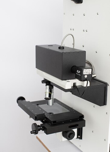
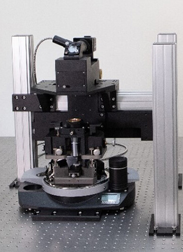
NTEGRA Spectra in upright configuration, “optics & spectroscopy”
NTEGRA Spectra in upright configuration, “optics & spectroscopy”
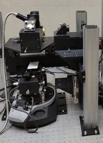
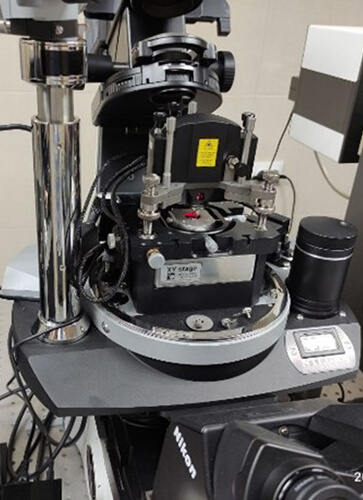
NTEGRA Spectra in upright configuration, SIO TOP and automated optical measuring head
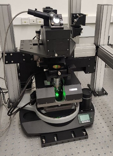
NTEGRA Spectra in upright configuration, combined SIO TOP & SIO SIDE, appropriate for TERS
NTEGRA Spectra in upright configuration, SIO TOP and manual optical measuring head NTEGRA
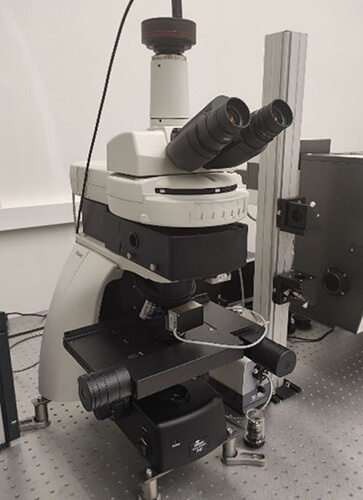
NTEGRA Spectra in inverted configuration on Olympus optical microscope
MEASURING MODES AND TECHNIQUES
Scanning probe microscopy
- Contact Atomic Force Microscopy (AFM)
- Amplitude modulation AFM
- AFM spectroscopy
- AFM lithography
- Jumping mode microscopy
- Lateral Force Microscopy (LFM)
- Force Modulation Microscopy (FMM)
- Spreading Resistance Imaging (SRI)
- Piezo Response Force Microscopy (PRFM)
- Electrostatic Force Microscopy (EFM)
- Kelvin Probe Force Microscopy (KPFM)
- Magnetic Force Microscopy (MFM)
- Scanning Capacitance Microscopy (SCM)
- Scanning Tunneling Microscopy (STM)
- STM spectroscopy
- STM lithography
- Scanning Thermal Microscopy (SThM)
- Photocurrent mapping
- AFM nanoindentation
- Electrochemical AFM
- Electrochemical STM
- “HYBRID” mode
Optical modes
- Confocal Fluorescence Microscopy
- Confocal Raman Microscopy
- Confocal Rayleigh Microscopy
- Near-Field Optical Microscopy
- Fluorecsence Lifetime Microscopy (FLIM)
- Fast-mapping Raman microscopy
- Laser confocal microscopy
- Dark Field Microscopy
- Polarization (white light) microscopy
- Optical contrasting microscopy
TECHNICAL DATA
| Scanning | |
| Scanning modes | by sample by laser beam both by sample and laser beam |
| Sample positioning | |
| Sample stage | motorized |
| Stage movement range | 130×80 mm (5×5 mm for SPM & combined measurements) |
| Sample weight and dimensions (in extended configuration) | |
| Sample size | up to Ø 40 mm × 10 mm |
| Sample weight | up to 100 g |
| Scanning by sample (in extended configuration) | |
| Scan range | 100×100×10 µm (±10%) |
| Non linearity, XY | ≤ 0.1 % |
| Noise level, Z (RMS in bandwidth 1 kHz) | ≤ 0.04 nm |
| Measuring head | |
| Deflectometer tuning | manual or automated |
| Deflectometer laser wavelength | choice of: 650 nm, 830 nm, 1300 nm |
| Optical parameters | |
| Objectives | magnification up to 100 X aperture up to 0.70 in the top channel (with probe holder installed) aperture up to 1.0 in the top channel (without probe holder installed) aperture up to 1.45 in the bottom channel |
| Diffraction gratings | up to 4 pcs. on the turret, to choose from: 150, 300, 600, 1200, 1800, 2400 gr/mm |
| Laser sources | |
| Quantity | up to 5 (4 built-in + one external) |
| Power | up to 120 mW |
| Wavelength range | from 400 to 800 nm |
| Polarization | linear |
| Beam profile | Gaussian TEM00, single longitudinal mode (SLM) |
| Monochromator entrance slit width | from 0 to 2000 µm step – 1 µm |
| Neutral density filters | ND=0.4 |
| Edge/notch filters | 8-position wheel, for filters Ø 12.5 mm and Ø 25 mm |
| Beam expander | optimized to fill out the objective lens pupil entrance |
| Calibration lamp | two-element hollow cathode |
| Detectors | CCD detector PMT (optional) APD (optional) |
KEY FEATURES
Optical spectroscopy
- Spectrometer with 3 or 4 diffraction gratings on a motorized turret
- Visible, near ultraviolet and near infrared spectral ranges
- Various detectors can be installed:
-
- CCD detector – for the visualization of the whole emission spectrum
- PMT or APD in photon counting mode for weak emission signals detection
- PMT for fast confocal laser (Rayleigh) visualization
-
- Motorized polarization optics in the excitation and the emission channels
- Motorized switching between laser lines
AFM/ STM integration with spectroscopy
- Upright and/ or inverted optical microscope
- Additional side channel for excitation and collection
- High-aperture optics to use simultaneously with AFM: up to 0.7 NA for upright, up to 1.45 NA for inverted version
- AFM/ STM and confocal Raman/ fluorescence images are acquired simultaneously being strictly colocalized
- All standard SPM imaging modes (more than 40) are available in combination with confocal Raman and photoluminescence microspectroscopy
- Minimal vibrations and thermal drifts due to special AFM optical heads design
- Sample surface is always in focus due to AFM Z feedback
- Atomic resolution in STM mode
Confocal microscopy and microspectroscopy
- Confocal Raman / photoluminescence / Rayleigh microscopy colocalized with AFM imaging
- Microspectroscopy spatial resolution close to the diffraction limit
- Motorized confocal aperture for spatial filtering of optical emission signal and high lateral and axial resolution
- 3D confocal imaging for transparent samples
- Beam expanders for the microscope objective entrance pupil optimal filling
- Point-by-point hyperspectral mapping of Raman and photoluminescence signals with further software analysis
- Optical lithography (vector, raster)
Optimization for tip-enhanced microspectroscopy (TERS, TEPL)
- All possible illumination and collection geometries for TERS/ TEPL are available: bottom, top and/ or side optical channels
- Various probe microscopy techniques and peculiar probes can be used to maximize gain: STM probes, AFM probes, quartz tuning fork probe in normal and shear force modes
- Scanning by sample/ by probe/ by laser spot to find out optimal focal point and to maximize probe enhancement
- Motorized polarization optics to adjust electric field direction of the incident light wave close to the nanoantenna probe
Software
- Seamless integration of probe microscopy and microspectroscopy; all AFM / STM / Raman / PL / SNOM experiments, data analysis and data processing in one software
- 1D, 2D and 3D hyperspectral mapping
- Data export to other formats (Excel, MatLab, etc.)